This a post about a book chapter:-
from a book on Natural Hydrogen Systems
Chapter 11 The development of an airborne, stand-off detection instrument for hydrogen gas
C. Ironside, M. Lynch, J. Martin, M. Paskevicius, M. D. Lorenzo, C. E. Buckley, et al.
In: Properties, Occurrences, Generation Mechanisms, Exploration, Storage and Transportation, edited by R. Rezaee and B. J. Evans
De Gruyter 2025
DOI doi:10.1515/9783111437040-011
https://doi.org/10.1515/9783111437040-011
The Hunt for Earth’s Hidden Hydrogen: How Lasers Are Unlocking a New Clean Fuel
A vast, untapped source of carbon-free energy may be seeping from the ground beneath our feet, and for a century, we have been almost entirely blind to it. Reports of natural hydrogen have existed for years, so if this clean fuel source is real, why haven’t we been using it?
The problem has been a technological one. For decades, we simply lacked the right tools to efficiently find these hydrogen deposits on a large scale. This article explores the surprising scientific and engineering breakthroughs that are finally allowing us to hunt for this hidden energy, not with drills and ground crews, but from the sky.
We Weren’t Finding It Because We Weren’t Really Looking
A primary reason natural hydrogen has remained an untapped resource is the lack of routine use of suitable detectors in geological exploration. Historically, the search has depended on handheld or fixed-point sensors—tools designed not for wide-area geological surveys, but for safety applications in hydrogen processing plants. These ground-based methods are inefficient for surveying the huge, often inaccessible areas where hydrogen might be seeping from the Earth.
This oversight is so fundamental that it has likely skewed our entire understanding of how much natural hydrogen is available. As a comprehensive 2020 review on natural hydrogen noted, the problem is a classic case of not having the right tools for the job:
“It is difficult to estimate how many times hydrogen has not been identified in H2 – rich samples because of the lack of a suitable detection technique to measure hydrogen concentrations.”
Why the Gas Industry’s Best Tools Are Blind to Hydrogen
The go-to technology for remote gas detection in the oil and gas industry is a form of laser-based radar called Differential Absorption LIDAR (DIAL). These systems are highly effective at spotting fugitive emissions of methane, but they are completely blind to hydrogen.
The reason lies in basic molecular physics. Molecules like methane (CH4) have a built-in electrical imbalance, known as a dipole moment. This property allows them to strongly absorb specific frequencies of infrared light, creating a clear signal that DIAL systems can detect from a distance.
Hydrogen (H2), however, is a homo-nuclear diatomic gas. Its two identical atoms share electrons perfectly, meaning it has no built-in dipole moment. Without this key characteristic, it doesn’t absorb infrared light in the same way. To the industry’s standard remote detection lasers, hydrogen is essentially invisible.
“Seeing” Hydrogen Means Finding One Photon in a Billion
To overcome hydrogen’s invisibility, scientists turned to a different physical principle: Raman scattering. When light from a laser hits a molecule, most of it bounces off with the same energy it arrived with, a phenomenon called Rayleigh scattering. However, a tiny fraction of that light interacts with the hydrogen molecule’s vibrations, stealing a bit of energy and bouncing off with a unique, lower-energy signature—its Raman fingerprint.
The challenge is that this signal is incredibly weak. At low hydrogen concentrations several meters from the instrument, the process is so inefficient that, for a given laser pulse, approximately 1 in 1,000,000,000 (1 × 10⁻⁹) of the laser’s photons are converted into the specific Raman photons that signal its presence. This fundamental difficulty—detecting an infinitesimally small signal from a vast sea of background light—is precisely why such a system wasn’t built sooner and why a major technological leap was required.
The Solution: A Flying, Photon-Counting Telescope
The breakthrough solution is an airborne system that combines lasers and highly sensitive optics into a technology called Time-Correlated Single Photon Counting (TCSPC) Raman LIDAR.
The concept involves an aircraft that scans the terrain below with a pulsed laser. A telescope, also mounted on the aircraft, collects the faint, backscattered light from the ground. The system is so sensitive that it can detect and precisely time the arrival of single photons returning from the target area. By filtering for the unique energy fingerprint of hydrogen’s Raman signal, this technology can map hydrogen concentrations on the ground with high specificity.
This airborne approach offers several powerful advantages over traditional methods:
• Speed and Scale: It can survey huge, inaccessible areas quickly, dramatically accelerating the exploration process.
• Precision: The system is highly specific to hydrogen, which reduces false positives and ensures accurate identification of seeps.
• Vertical Profiling: It can create 3D maps of a hydrogen plume, helping to trace it back to its source on the ground.
• Integration with Other Sensors: The hydrogen data can be combined with magnetic, gravitational, and electromagnetic surveys to build a comprehensive geological picture.
• Real-time Data: It enables scientists to collect and process data immediately, facilitating analysis and decision-making during survey flights.
• Non-Invasive: As a remote-sensing method, it doesn’t require physical contact with the ground, preserving the natural environment.
A Working Lab Prototype
This advanced detection technology is not just theoretical. Researchers at Curtin University have developed and tested a laboratory-based proof-of-concept instrument to validate the TCSPC Raman LIDAR approach.
The lab tests were a success. The prototype demonstrated a limit of detection (LOD) of 9,000 parts per million (ppm) at a distance of 2 meters. Critically, achieving this sensitivity required a 60-second integration time.
This result validated the team’s numerical model, which they are now using to design the final airborne instrument. The next phase of the project highlights the immense engineering challenge ahead, with an ambitious but necessary target: to develop an airborne system capable of achieving an LOD of 1,000 ppm at 50 meters with a 0.1-second integration time. Reaching this level of performance is essential for effective and rapid aerial exploration.
A New Era of Energy Exploration
For decades, a potentially massive source of clean energy has remained largely ignored, not because it wasn’t there, but because we lacked the ability to see it. Now, thanks to a technological leap from handheld sensors to flying, photon-counting telescopes, we are on the cusp of being able to map Earth’s natural hydrogen resources for the first time.
As this technology moves from the lab to the sky, its impact will extend far beyond initial exploration. This same capability will be crucial for monitoring the broader hydrogen economy, enabling activities ranging from fugitive emission monitoring and environmental impact assessments to ensuring that industrial facilities comply with safety regulations. A tool designed to find a hidden fuel may soon become essential for managing our energy future.
This post is about the paper:-
X. Sun, W. D. A. Rickard, O. S. Burrow, E. Riis, and C. N. Ironside, “Investigation of nanofabrication on (111), (100) and (110) surfaces of single-crystal aluminium,” Next Research, p. 101202, 2025/12/06/ 2025,
https://www.sciencedirect.com/science/article/pii/S305047592501067X?via%3Dihub
The Unexpected Champion: How One Crystal Orientation Unlocks Flawless Aluminum
1.0 Introduction: The Hidden Problem with Everyday Aluminum
Aluminum is one of the most common and useful metals in the world. We find it everywhere from kitchen foil to aircraft fuselages. But for the demanding world of high-tech optics, the standard form of this familiar metal has a major flaw. When scientists and engineers try to shape and pattern regular, or “polycrystalline,” aluminum for advanced applications, they run into a persistent problem: surface roughness.
This roughness, a natural result of the metal’s microscopic crystal structure, limits its use in high-precision components like mirrors and gratings for visible, ultraviolet, and extreme ultraviolet (EUV) light. For technologies like quantum computing and advanced sensors, even a few nanometers of roughness can ruin performance. This raises a critical question for material science.
What if we could create perfectly smooth aluminum surfaces? What secrets would we have to unlock at the atomic level to do it? A new study investigates this very problem, exploring how different fabrication techniques interact with aluminum’s fundamental atomic structure to either create a flawlessly smooth surface or a chaotically rough one.
2.0 Takeaway 1: Not All Aluminum is Created Equal
1. Your Kitchen Foil Isn’t Smooth Enough for a Quantum Computer
The aluminum in your kitchen is polycrystalline, meaning it’s composed of countless microscopic crystal grains all oriented in random directions. When you try to sculpt this type of aluminum on a nanoscale, these random grains create a messy, uneven surface. In contrast, single-crystal aluminum is a pristine, perfectly ordered material where all the atoms are aligned in a single, continuous lattice.
This fundamental difference becomes starkly clear when subjected to nanofabrication techniques like Focused Ion Beam (FIB) milling or Reactive Ion Etching (RIE). The research highlights the “well-known rough surface morphology issue with polycrystalline Al alloys.” Visual evidence from the study’s microscope images shows the stark difference: the polycrystalline aluminum surface appears coarse and pebbled after processing, while the single-crystal surfaces are dramatically cleaner. This proves that the key to a perfect surface begins with a perfect crystal.
3.0 Takeaway 2: The Crystal’s Orientation is the Key to Perfection
2. A Crystal’s “Face” Determines Its Fate
Even within a perfect single crystal, not all surfaces are the same. The arrangement of atoms can be exposed in different ways, creating distinct planes or “faces.” The researchers investigated three of the most important crystallographic orientations, designated as (111), (100), and (110). Think of these as looking at the crystal’s atomic structure from three different angles.
The study discovered that the results of the fabrication process were “strongly dependent on the crystallographic orientation of the Al.” The speed of the process and the final smoothness of the surface could be changed dramatically simply by choosing a different crystal face to work on. This finding revealed that controlling the final surface quality isn’t just about using a single crystal, but about choosing the right face of that crystal.
4.0 Takeaway 3: And the Winner Is… The (110) Surface
3. The Unexpected Champion for Smoothness and Speed
After testing all three orientations with different techniques, the research identified one clear winner. When using the chemical Reactive Ion Etching (RIE) method, the single-crystal aluminum with a (110) orientation vastly outperformed the others.
The data points tell a compelling story. The Al (110) surface delivered an unparalleled surface roughness of just 2±0.5 nm. To put that in perspective, this result is 2 to 4 times smoother than the other surfaces tested with the same technique: the (111) face (4±0.5 nm), the (100) face (6±0.5 nm), and standard polycrystalline aluminum (8±0.5 nm). On top of its winning smoothness, it also had the highest etch rate at 15±2 nm/min.
This combination of speed and smoothness makes the (110) orientation a highly promising substrate for creating the next generation of “low-loss diffractive optical elements,” where even the slightest imperfection can scatter light and degrade performance. The study suggests a reason for this success: the (110) surface has the highest surface energy. Think of surface energy as a measure of how “unstable” or reactive the atoms on the surface are. The higher energy of the (110) face makes its atoms more susceptible to the chemical etching process, allowing them to be removed more quickly and cleanly.
4. A Warning: The Precision Tool That “Poisons” the Metal
Focused Ion Beam (FIB) milling is a powerful tool in nanofabrication. It acts like a microscopic sandblaster, using a precise beam of gallium ions (Ga+) to carve out tiny, intricate patterns, making it excellent for “rapid prototyping.” On certain crystal faces, its performance is remarkable; for instance, on the Al (111) surface, FIB milling is incredibly fast (52 nm/min) and produces a very smooth surface (2 nm).
However, this performance comes at a cost: the unavoidable “poisoning” of the surface with gallium. The high-energy gallium ions don’t just carve the aluminum; they get implanted into it. This contamination causes “liquid metal embrittlement,” which fundamentally weakens the material. Specifically, the embedded gallium disrupts the formation of the naturally protective layer of aluminum oxide. This naturally-forming oxide layer is aluminum’s armor, protecting it from corrosion. By disrupting it, the FIB process fundamentally compromises the long-term stability and integrity of the material, a crucial flaw for sensitive optical components. This creates a critical choice for engineers between initial fabrication speed and the final material’s integrity, where RIE emerges as the safer, cleaner option for high-performance optics.
6.0 Conclusion: From a Simple Metal to a High-Tech Future
This research provides a clear and practical roadmap for fabricating ultra-smooth aluminum surfaces for advanced optical devices. By pairing the right material—single-crystal aluminum—with the right atomic orientation—the (110) face—and the right technique—Reactive Ion Etching—scientists can overcome the long-standing challenge of surface roughness.
The impact of this work is best summarised by :
This enhanced understanding of how crystal orientation affects surface quality is expected to contribute significantly to the advancement of low-loss diffractive optical elements across the infrared to extreme ultraviolet spectral ranges.
Introduction: Beyond Empty Space
Here are some the concepts from my recent paper :-
H. Taya and C. Ironside, “Kramers-Krönig approach to the electric permittivity of the vacuum in a strong constant electric field,” Physical Review D, Article vol. 108, no. 9, p. 28, Nov 2023, Art no. 096005, DOI:10.1103/PhysRevD.108.096005.
https://journals.aps.org/prd/abstract/10.1103/PhysRevD.108.096005
They do say that the drawback of specialisation is that the specialised “knows more and more about less and less” – until we arrive at knowing everything about nothing – the vacuum.
What is a vacuum? For most of us, the answer is simple: it’s empty space, the vast nothingness between stars and galaxies. But at the most fundamental level, this couldn’t be further from the truth. Quantum mechanics paints a far stranger picture, one first envisioned by the brilliant physicist Paul Dirac. He theorized that the vacuum is not empty at all, but a roiling, energetic sea of potential particles.
At the quantum level, Dirac predicted that the vacuum of quantum electrodynamics (QED) is not just empty space, and has a structure similar to the semiconductor, called the Dirac sea.
This “Dirac sea” is constantly simmering with electron-positron pairs that can pop into existence and annihilate in the blink of an eye. This raises a profound question: What happens when you apply an extremely powerful electric field to this “not-so-empty” space? A new study reveals some deeply counter-intuitive answers, drawing a stunning parallel between the cosmos and the components inside our everyday electronics.
1. The Big Idea: The Vacuum Is a Semiconductor
The core insight of the paper is a powerful analogy: the QED vacuum’s “Dirac sea” of potential electron-positron pairs is functionally similar to the “valence band” of electrons in a semiconductor material. In a semiconductor (like the silicon in a computer chip), electrons in the valence band are locked in place, but a strong enough electric field can jolt them free, allowing electricity to flow.
Similarly, a strong enough electric field can jolt the vacuum, causing it to exhibit surprising new properties. This analogy isn’t just a clever comparison; it’s a practical tool. As the researchers note, it allows physicists to “import the wisdom of semiconductor physics to strong-field QED” and predict how the fabric of reality itself might behave under extreme conditions.
2. Shocking the Void: Creating Matter from Nothing
One of the most mind-bending predictions of strong-field QED is the Schwinger effect: the idea that an incredibly strong electric field can literally tear electron-positron pairs out of the vacuum, spontaneously creating matter from what appears to be nothing. This is the cosmic equivalent of the “dielectric breakdown” of a semiconductor, where a strong field causes an insulator to suddenly conduct electricity.
However, the field strength required for the Schwinger effect is astronomical—Ecr = 1.32 × 10¹⁸V/m—a level far beyond what we can currently generate. The new research highlights a clever workaround known as the “dynamically assisted Schwinger effect.” This technique proposes using a combination of a strong, constant electric field and a weaker, oscillating “probe” field (like a laser). Together, they can significantly boost the rate of pair production, potentially bringing this exotic phenomenon within reach of near-future laser technology. This is the QED version of a well-known phenomenon in electronics called the Franz-Keldysh effect, which is already used in real-world technologies like “electroabsorption modulators… widely used in high-speed digital communications.”
3. A Unified View: The Glow of Creation and the Bending of Light
The research establishes a critical link between two seemingly separate phenomena: the creation of matter and the optical properties of the vacuum. The authors established a “quantitative correspondence between the electric permittivity and the number of electron-positron pairs produced.”
In simple terms, this means that the experiments have two distinct ways to verify the theory, and one confirms the other:
• The “absorptive” property of the vacuum, described by the imaginary part of its permittivity, is directly tied to the rate at which matter (electron-positron pairs) is created.
• This means scientists could either measure how the probe light is bent and absorbed as it passes through the strong field, or they could directly measure the particles being created. Finding one is proof of the other.
As the paper states, this provides a powerful experimental link:
…the observation of the pair production can be used to directly quantify the response function of the QED vacuum, i.e., the imaginary part of the electric permittivity and in turn the real part through the Kramers-Krönig relation.
4. A Birefringent Void: The Vacuum Can Split Light Like a Crystal
One of the most profound implications of this research is that under a strong electric field, the vacuum itself becomes birefringent. Birefringence is a property seen in certain crystals, like calcite, where the material has a different refractive index depending on the polarization of light passing through it. This causes the crystal to split a single beam of light into two.
The study confirms that a strong electric field forces the vacuum to behave in the same way. The vacuum’s response is different for a probe field polarized parallel to the strong field (ϵk) versus one that is polarized perpendicular to it (ϵ⊥). The profound takeaway is that an intense electric field imposes a “direction” or “grain” onto the fabric of spacetime itself, causing it to treat light differently based on its orientation, just like a crystal.
Conclusion: The Future of a Structured Vacuum
This research powerfully reinforces that the vacuum is not a passive void, but a complex, structured medium whose properties can be altered and probed. By applying the principles of semiconductor physics to quantum electrodynamics, physicists have discovered a direct link between the bending of light and the creation of matter, revealing an underlying oscillating rhythm in the vacuum’s structure. These insights pave the way for future high-power laser experiments that could “quantitatively diagnose the QED vacuum” and may one day help us understand extreme physical systems like heavy-ion collisions and compact stars.
As we get closer to creating and manipulating the vacuum’s properties, are we simply observing the universe, or are we learning to write on its most fundamental canvas?
Went on an excellent dive trip to the remote Rowley Shoals in Western Australia between 30/11/20-05/12/20 – Rowley shoals is about 300km northwest of Broome in Western Australia. Went with the dive boat the Great Escape The boat sets off from Broome and travels overnight to Rowley shoals. We encountered some rough seas and some of the passengers were seasick but arrived safely at our destination.

Day1
It’s a very remote location and the fish don’t get many visitors so they are curious about the SCUBA fish that blow bubbles. Check out this puffer fish.
I had the very annoying experience with my Atomic Cobalt 2 dive computer failing again after it had been “repaired” by Atomic. The Great Escape crew were excellent and quickly came up with a workaround. They lent me a simple pressure gauge.
Heres’ a white tipped reef shark resting on the sandy bottom and being cleaned
Day 2 of the great escape
Another view of a white tip


There were a lot of massive bump head parrot fish and reef sharks.
Day 3 & 4 of the great escape
A bump head getting cleaned by two cleaner wrasse
The eye of the clown fish

The coral rhino head

The dazzling smile and impressive, coral munching, teeth of the bumped parrot fish


The Clown fish don’t like to leave their anemone and so they are easy to photograph and video.
We headed back to Broome after the 4th day. We just missed a storm which arrived the day after we got back to Broome.
Authors:
Charlie Ironside,Department of Physics and Astronomy, Curtin University, Bentley, Western Australia
Bruno Romeira,Department of Nanophotonics, Ultrafast Bio- and Nanophotonics group,
INL – International Iberian Nanotechnology Laboratory, Av. Mestre José Veiga s/n,
4715-330 Braga, Portugal
Jose´ Figueiredo,Department of Physics of the Faculty of Sciences at University of Lisbon, Campo Grande,
1740-016 Lisboa, Portugal
Morgan
Check out :-https://iopscience.iop.org/book/978-1-64327-744-8
Quantum Effects Building the Future of Electronics
Introduction: Beyond Moore’s Law
For decades, the relentless march of technology has been powered by a simple principle known as Moore’s Law: the number of transistors on a chip doubles roughly every two years, making our computers faster and more powerful. But that march is slowing. As components shrink to near-atomic scales, the bizarre rules of quantum mechanics begin to interfere, making further progress with traditional designs incredibly difficult. As the demand for “beyond Moore’s law technologies” becomes urgent, a new approach is emerging.
Instead of fighting the strange effects of quantum mechanics, scientists are now learning to harness them. They are building a new generation of devices that operate on principles that seem to defy common sense. A prime example of this new paradigm is the Resonant Tunnelling Diode (RTD), a semiconductor device whose incredible speed and functionality are derived directly from the counter-intuitive nature of the quantum realm. By embracing these bizarre effects, we are not just pushing the limits of electronics—we are rewriting the rules entirely.
——————————————————————————–
1. To Help Electrons Flow, Add Another Wall
The first quantum trick sounds like a paradox: to make it easier for an electron to pass through an energy barrier, you should add a second one right behind it. In classical physics, this is like trying to run through two walls instead of one—it should be harder, not easier. But in the quantum world, particles like electrons also behave like waves. In a single-barrier setup, the probability of an electron “tunnelling” through is vanishingly small across almost all energy levels. But by adding the second barrier, a sharp, narrow “transmission peak” emerges, where the probability of tunnelling for an electron with the perfect resonant energy shoots up dramatically—in some cases approaching 100%.
This happens because the two parallel barriers create a tiny space—a quantum well—between them. Think of it like a guitar string. A string of a specific length will only resonate powerfully at a specific frequency (a musical note). The quantum well acts like that fixed length, and only electrons with the corresponding “frequency”—the correct energy—can resonate and pass through. All others are simply turned away. This highly selective resonance is the core principle of the Resonant Tunnelling Diode.
This leads to the somewhat counter-intuitive conclusion that adding an energy barrier increases the probability of transmission through the structure at energies below the height of the barrier.
This effect is a foundational quantum trick. It doesn’t just allow electrons to pass through “impassable” walls; it allows engineers to precisely control electron flow at the quantum level, enabling the powerful behaviors that follow.
——————————————————————————–
2. Get More by Pushing Less: The Power of “Negative Resistance”
In every electronic device you own, the relationship between voltage and current is simple: push with more voltage, and you get more current. The Resonant Tunnelling Diode, however, has a region in its operation where it does the exact opposite. This property is known as Negative Differential Conductance (NDC), where increasing the voltage across the device paradoxically causes the current flowing through it to decrease. This is not just a curiosity; it means that in this operational range, the device defies the normal rules of resistance. Instead of consuming energy, it actively generates RF power, making it a nanoscale engine for ultra-high-frequency signals.
This strange electrical behavior is the key to the RTD’s extraordinary performance. In this NDC region, the device isn’t absorbing power like a typical resistor; it is actually generating power, giving it “electrical gain.” This ability to amplify signals at incredibly high speeds is a direct result of the quantum tunnelling mechanism.
The impact of this property is profound. By harnessing negative resistance, RTDs can act as the fastest electronic oscillators ever built at room temperature. Electronic oscillators based on this principle have been demonstrated to operate at frequencies up to an incredible 1.93 THz. To put that in perspective, 1.93 THz is nearly 1,000 times faster than the gigahertz clock speeds of today’s top-tier computer processors.
——————————————————————————–
3. It Thinks, Therefore It Is: Building an Artificial Neuron
The complex, highly nonlinear behavior of the RTD bears a striking resemblance to a fundamental biological process: the firing of a neuron. As far back as the 1960s, scientists used a similar device, the Esaki tunnel diode, to create an electronic circuit that could simulate a nerve axon. Today, this concept has evolved into a key strategy for building “neuromorphic” or brain-like computing systems.
Modern RTD-based devices, which can be integrated with tiny lasers or photodetectors, can produce sharp “spikes” and “bursts” of signals that mimic the action potentials of biological neurons. This behavior is called “excitability” and is characterized by an “all-or-none response.” An input signal below a certain threshold produces a tiny, negligible effect. But an input that crosses that threshold triggers a large, standardized output pulse, exactly like a neuron firing. This capability is the foundation for neuromorphic photonic computing, which aims to process information with the efficiency and style of the human brain.
This ability to build a device that fires like a neuron is a direct consequence of engineering at a very specific physical size. As Nobel laureate Alain Aspect explained, this is the realm of the mesoscopic:
‘between the scale of a single atom and the macroscopic world, one finds the mesoscopic scale, where it is the object itself, and not only the material of which it is made, that needs to be described by quantum mechanics’
— Alain Aspect
The RTD is not just made of quantum materials; at the mesoscopic scale, the device itself is a quantum object, and its bizarre, neuron-like behavior is the result.
——————————————————————————–
Conclusion: The Quantum Leap Forward
The future of high-speed electronics is being built on principles that defy our everyday intuition. By adding a second barrier to help electrons flow (resonant tunnelling), pushing with more voltage to get less current (negative resistance), and building devices that fire like brain cells (excitability), scientists are moving beyond the limits of classical physics.
This represents a fundamental paradigm shift. For half a century, we treated quantum weirdness as a bug to be squashed. Now, we’re deploying it as the ultimate feature, building an entirely new class of electronics that thinks, oscillates, and computes in ways classical physics deemed impossible.
The second edition of my book “Semiconductor Integrated Optics for Switching Light” has just been published (May 2021). Check out:-https://iopscience.iop.org/book/978-0-7503-3519-5 It’s a book on using semiconductor optical waveguides for controlling light. It provides a concise description of the physics and engineering of semiconductor optical waveguides for photonic and electronic switching with a focus on optical communication applications. It provides Python notebooks that illustrate the concepts discussed in the book. The book includes the following topics: linear and nonlinear optics, linear electro-optic effect electroabsorption and electrorefraction, nonlinear refraction, nonlinear optical devices.
There is supporting material in the form of a youtube video
There are are Python and Mathematica notebooks that can be used to help with the design of some of the devices discussed in the book.
Python notebooks at :-https://doi.org/10.5281/zenodo.4506293
Mathematica notebooks:-https://doi.org/10.5281/zenodo.4448672
Enjoy!

thick Al0.25Ga0.75As. The active layer is thick Al0.18Ga0.82As. The cladding layer is thick Al0.25Ga0.75As. The mesa strip is wide and in height. The approximate position of the guided light at the facet is indicated by the red area.
Why Your Computer Isn’t Getting Faster—And How Photonics Could Break the Deadlock
Introduction: The Speed We Can’t Use
For decades, we took for granted that computers would get exponentially faster every year. But if you’ve bought a new computer recently, you might have noticed something strange: the raw clock speed of its processor probably isn’t much faster than the one you had a decade ago. Since around 2004, the core clock speed of microprocessors has been largely stuck in the 3–5 GHz range. We’ve added more cores and clever software tricks, but the fundamental clock frequency of the processor has hit a wall.
The surprising reason for this stagnation isn’t that we can’t make transistors switch faster. The real culprit is thermodynamics. The dominant technology in computing, known as CMOS, has a primary weakness in heat management. Every time a transistor switches to process a ‘1’ or a ‘0’, it generates a tiny puff of heat. At billions of operations per second, those puffs add up to a thermal inferno that we simply can’t cool down fast enough. We’ve reached the physical limit of how much heat we can remove from a chip.
To break this deadlock, researchers are exploring a radical solution: getting rid of the electrons and switching with light itself. This field, known as all-optical switching, uses photons to process information. By using light to control light, it may be possible to bypass the thermal bottleneck that has plagued electronics for years, unlocking a new era of computational speed.
——————————————————————————–
1. The Real Enemy of Speed Is Heat, Not Time
The fundamental limit of modern computing is a law of physics. The second law of thermodynamics states that every switching operation increases entropy, or disorder. In the electronic world of CMOS chips, this increase in entropy inevitably ends up as waste heat. We’ve become so efficient at packing transistors onto silicon that we’ve reached a point where the heat generated can’t be dissipated quickly enough, limiting how fast we can run the chip.
The core problem is elegantly stated in research on the topic:
If CMOS does have any weakness it may be in the heat management associated with ultrafast switching.
The issue is not just the total amount of heat, but the physical speed limit at which a material can shed it. The industry is stuck with the thermal diffusion coefficient of silicon, a fundamental property that dictates how quickly heat can move through the material. This creates a hard physical ceiling on processing speed.
All-optical switching offers a clever way around this problem. In certain forms of optical computing, the entropy “price” for a switching operation is still paid, but it “does not end-up in heat.” Instead of heating the material, the cost of the operation is paid in more subtle ways—for instance, as the physics of these interactions shows, it can manifest as an increase in the phase uncertainty of the light itself.
This reframes the entire challenge of high-speed computing. The problem isn’t just about achieving raw speed; it’s about managing energy and heat. By shifting from electrons, which generate heat when they move, to photons, which can process information without thermal buildup, we open an entirely new path forward.
——————————————————————————–
2. You Can Steer a Beam of Light With Another Beam of Light
The central principle behind all-optical switching lies in a field called nonlinear optics. Normally, we think of materials like glass as having fixed optical properties—light passes through without changing the glass itself. However, at sufficiently high intensities, light can actually alter the optical properties of the material it’s traveling through.
One of the key mechanisms is the “optical Kerr effect,” where the intensity of a light beam changes the material’s refractive index (the property that determines how much the material bends light). A high-intensity pulse of light can essentially make a pathway temporarily more or less “optically dense” for other light passing through it.
Researchers use this principle to build devices like a “nonlinear directional coupler.” Think of two microscopic waveguides as two parallel lanes of a highway built from a special material. At low traffic volumes, cars (light pulses) naturally drift from the first lane into the second over a short distance. But a high-intensity “control” pulse is like a sudden, temporary change in the road surface of the first lane, making it ‘stickier’ and preventing any cars from drifting across. The control pulse creates a temporary barrier with light itself. In effect, the control beam of light acts as a switch, steering the data beam.
This all happens without any electronic-to-optical conversion, allowing for incredible speeds. Because the effect relies on the near-instantaneous response of bound electrons in the material, the ultimate switching speed limit is in the attosecond (a billionth of a billionth of a second) range. This is millions of times faster than the gigahertz clock speeds of today’s best processors, operating on a timescale where we can influence the very oscillation of a light wave itself.
——————————————————————————–
3. To Build the Perfect Switch, You Need the “Imperfect” Material
Building a practical all-optical switch presents a significant challenge. You need a material with a large nonlinear refractive index—the property that allows a control pulse to strongly affect a data pulse. At the same time, you must avoid a phenomenon called “two-photon absorption.” This is a process where the material absorbs two photons at once from the high-intensity control pulse, which wastes energy and, crucially, generates the very heat you’re trying to avoid.
The solution is a masterpiece of materials science. Using a semiconductor alloy called Aluminum Gallium Arsenide (AlxGa1−xAs), engineers can “tune” the material’s properties by precisely adjusting the aluminum fraction (the ‘x’). For the wavelengths used in optical communications (around 1550 nm), researchers discovered a “sweet spot.”
The ideal material isn’t a pure element but a precisely formulated alloy: Al₀.₁₈Ga₀.₈₂As. This specific composition adjusts the material’s electronic bandgap—the minimum energy required to excite an electron. The material is engineered so that the energy of a single photon is less than the bandgap, preventing it from being absorbed on its own. Crucially, the photon energy is also engineered to be less than half the bandgap energy. This makes it energetically impossible for two photons to combine their energy to excite an electron, thus eliminating two-photon absorption. This “just right” configuration maximizes the useful switching effect while minimizing wasteful, heat-generating absorption. It’s a powerful example of how quantum mechanics can be used to engineer a material with the exact compromise of properties needed to build a new technology.
——————————————————————————–
4. Running Absorption Backwards Could Create a New Kind of Laser
Physics often has a beautiful symmetry. The same process that can be an undesirable side effect can sometimes be flipped on its head to create a powerful new tool. The problem of “two-photon absorption” has an inverse: “two-photon gain.”
Under normal conditions, a material can absorb two photons at once. However, if you pump the material with external energy—similar to how a conventional laser works—you can create a “population inversion” (a state where more electrons are in a high-energy state than a low-energy one, making the material eager to release energy rather than absorb it). In this energized state, the process reverses. Instead of absorbing two photons, an incoming photon can stimulate the material to emit two highly correlated photons simultaneously.
This phenomenon could be the key to building a “two-photon semiconductor laser.” Such a device would be an entirely new kind of light source capable of producing the ultrashort, high-intensity pulses of highly correlated photons that are required for high-speed, all-optical processing. While a practical two-photon semiconductor laser has yet to be fully realized, the principle shows how even the physical limitations in one area can become the foundation for groundbreaking technology in another.
——————————————————————————–
Conclusion: A New Light for Computation
To continue advancing the speed of information processing, we may need to fundamentally shift our tools from electrons to photons. All-optical switching bypasses the thermal limits of today’s electronics by using light to control light, a process that can occur on timescales thousands of times faster than current processors without generating waste heat.
From the realization that heat, not time, is the true barrier, to the engineering of “imperfect” materials with perfectly balanced quantum properties, the path toward optical computing is illuminated by surprising and elegant physics. Even parasitic effects like two-photon absorption can be inverted to create new technologies like two-photon lasers.
While significant engineering challenges remain, the physics is clear. The question is no longer if we can build computers that run on light, but what new worlds will we discover when computation can happen on the timescale of a single light wave? The answer could redefine everything from artificial intelligence to drug discovery, opening up computational frontiers that today exist only in theory.
Dewi Nusantara is a liveaboard SCUBA diving boat operating in Indonesia. We were on this boat in September 2019 on a Raj Ampat trip out of Sorong in West Papua, Indonesia. Top of the range dive boat and trip – exceptionally healthy reefs.
Here are some highlights
Pygmy sea horse on fan coral

Manta ray just passing by:-
Feeding fish – I stirred up some sand for the benefit of the bottom feeders:-
The symbiotic relationship between a Goby and a Pistol Shrimp -very happy couple:-
A big bump head fish feeding on coral.

This is a picture taken underwater looking up at the sky and it shows the Snell’s window effect. The Snell’s window is the bright central region of the photograph- it is quite a well-known phenomenon and the dark region at the edge of the photograph is sometimes called Snell’s blanket and that’s when the angle of incidence of the light on the surface of the water is such that no light penetrates the water. It is related to the critical angle for total internal reflection. An easier way to understand this problem is to envisage a point source of light at a depth z in the water -so this inverts the problem but that is ok because the laws of optics are reversible.
The inverted problem about how light escapes from a high refractive index material to a low refractive index material is related to the extraction efficiency of light emitting diodes (LEDs) – in the LED the light is generated inside a semiconductor typically with a refractive index, n1~3.5, and has to escape from the semiconductor into the air with n2=1.0003. Extraction efficiencies can be low because of the large refractive index of semiconductors.
The amount of reflection and transmission at a surface is governed by Fresnel equations. The input parameters into Fresnel equations are the angle of incidence, the refractive index of media and the polarisation of the light. The other consideration is Snell law that gives the relationship between the angle of incidence and the angle of transmission (or refraction) and from Snell’s law, the critical angle for total internal reflection can be determined.
The photograph was taken with a surface between the water and the air which was not perfectly smooth there are ripples on the surface of the water. But to apply Fresnel’s equation to get an insight into the physics behind Snell’s window we are going to assume a perfectly smooth surface. Further in the photograph, we are looking up at the sun and the rays of light are coming in from a particular direction – in our modelling we are going to assume that the light is coming with equal probability from all directions in the celestial hemisphere. The kind of condition approximately by a very cloudy sky what I am going to call a Lambertian sky.
So Fresnel equations, give the fraction of light reflected at a surface between to media with refractive index 

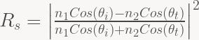


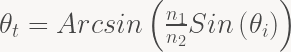
So to explain the Snell’s window in the photo we need to take account of the fact that the angle incidence at the surface (the x-y plane) for a viewer from a depth of z is given by :-
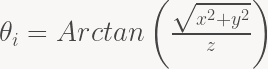
To help visualise the Snell’s window we can use the density plot function in Mathematica and we code the above equations to get the following :-

This for unpolarised light (an average of s and p polarized light) looking up from a depth of 5 meters (the x and y scales are in metres) the refractive index of the water is n1=1.33 and air n2 =1.00 – we assume a perfectly flat surface and light coming from all -directions with a Lambertian sky. It sort of captures the essence of the Snell’s window effect – although it might be more appropriate to call this the Fresnel’s window. Brewster’s angle is the angle at which p polarised light is transmitted with zero loss – there is no equivalent for s -polarised light and it means that under the sea the light is partially polarised.
If you would like to play around with different refractive indices and depths then check out the Snell’s Window simulation So the different refractive indices are appropriate to figuring out the extraction efficiency from LEDs and indeed the injection efficiency into solar cells.
Below is a movie of how Snell’s window at the surface changes as depth increases – it assumes n1=1.33 the refractive index of water:-
The movie below shows how Snell’s window at the surface changes as the refractive index n1 increases – so that it shows how less light escapes from the material as the refractive index increases – it relates to how light escapes from an LED – the depth is 4 microns and the x-y scale is in microns.
Should you ever find yourself having to calculate the refractive index of the semiconductor alloy Aluminium Gallium Arsenide, AlxGa1-xAs – so that’s the alloy with an Aluminium fraction of x. Then click here to see the refractive index as a function of wavelength.
VCSELs (see Brtiney Spear’s take on VCSELs http://britneyspears.ac/physics/vcsels/vcsels.htm )are components in the 3D face recognition system used in the later versions of the iPhone – the VCSELs generate the structured light required to obtain the 3D information from a scene see https://appleinsider.com/articles/18/03/08/apple-vcsel-supplier-suggests-truedepth-coming-to-multiple-iphones-this-fall. They are also used in miniature atomic clocks https://www.photonics.com/Articles/VCSEL-driven_Atomic_Clock_Available_to_Consumers/a46948
The VCSELs include an electrically insulating oxide layer that is used to channel the current in the device. Fabricating the oxide layer is an important part of the VCSEL manufacturing processes and by using a nanoanalysis technique called FIB-ToF-SIMS the atomic species in the device can be 3D mapped with a resolution down to a few nanometers. At the John De Laeter centre of Curtin University, we used FIB-ToF-SIMS to analysis the atomic species in a VCSEL manufactured by Compound Semiconductor Technologies. With FIB-ToF-SIMS we can precisely map out the oxide layer in the VCSEL and determine if it is up to specifications.
When we map out the atomic species of interest in even a small volume we end up with a lot of data – in the movie shown below we show the Gallium, Aluminium and Oxygen atoms in cube volume device 2x2x2 microns – of particular interest is the lower Oxygen atoms -shown in red in the Aluminium oxide layer – the oxide layer on top is a SiO2 protection layer – not really that important for device operation.
Enjoy the movie:-
